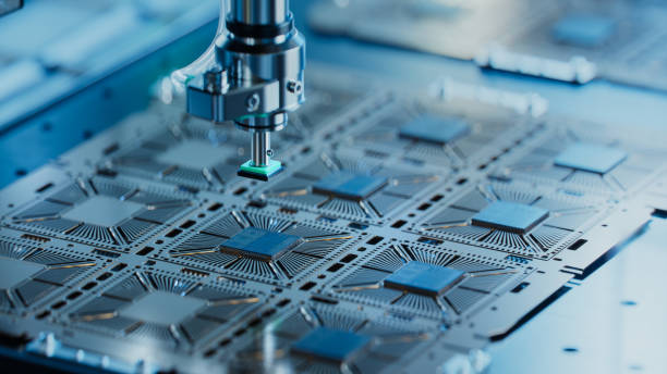
QUICK ANSWER: PCB assembly (PCBA) is the process of populating a bare printed circuit board with electronic components, soldering those components in place, and validating the finished board through electrical testing. It is distinct from PCB fabrication, which produces the bare substrate. A complete PCBA process covers SMT placement, reflow soldering, through-hole soldering where needed, inspection, and functional test.
A lot of companies send Gerber files to a PCB assembler and wait for working boards to come back. That works until it doesn’t. When boards arrive with open solder joints under a BGA package, or a wrong-value resistor pulls the output voltage out of spec, the conversation about what the assembly process actually involved becomes very expensive.
That sounds obvious, but most buyers skip the process audit and just compare per-board pricing. The assemblers who quote cheapest are often the ones who skip automated optical inspection or skip electrical test entirely. You don’t find out until field failures start showing up.
Understanding what happens between bare board in and tested assembly out tells you exactly what to ask, what to require, and what a legitimate PCB assembly provider should be able to demonstrate.
From Bare Board to Tested Assembly: The Full Process
PCBA is a sequence of steps, not a single operation. Each step introduces potential failure modes, and each step requires either automated or human verification to catch defects before they compound.
Solder Paste Printing
The process starts with solder paste deposition. A stainless steel stencil with apertures matching the PCB’s SMT pad locations gets aligned over the board, and a squeegee deposits solder paste through the openings. The paste is a mix of tiny tin-silver-copper alloy spheres suspended in flux.
Paste volume is critical. Too little paste and the joint won’t form. Too much and you get bridging between adjacent pads, which is a particular problem on fine-pitch QFP packages and 0402 passives. Automated solder paste inspection (SPI) systems measure paste volume and alignment on every board before any components go down. Assembly houses that skip SPI are gambling on every panel.
Pick-and-Place Component Placement
Pick-and-place machines lift components from tape-and-reel or tray feeders and place them on the solder paste with position accuracy measured in hundredths of a millimeter. Modern SMT placement equipment like Fuji NXT or Panasonic NPM lines can place tens of thousands of components per hour.
Here’s the thing most people miss: feeder setup verification matters as much as placement speed. A component placed from the wrong feeder, say a 10k resistor landed in a spot designated for 1k, won’t cause a placement error the machine flags. It just makes a board that fails test. That’s why incoming component verification against the bill of materials, and barcode-matched feeders, are process controls that separate serious assemblers from low-cost shops.
Reflow Soldering
The populated board travels through a reflow oven, passing through preheat, soak, reflow, and cooling zones. The temperature profile must ramp and hold within tolerances specified by the solder paste manufacturer. A typical SAC305 (tin-silver-copper) lead-free process peaks at around 245-260 degrees Celsius in the reflow zone.
Lead-free soldering under RoHS compliance is now standard for most commercial and consumer electronics. HASL (hot air solder leveling), ENIG (electroless nickel immersion gold), and OSP (organic solderability preservative) are common PCB surface finishes that affect solder joint quality. ENIG is preferred for fine-pitch components because of its flat, co-planar surface; HASL works fine for most through-hole and larger-pitch SMT applications.
Through-Hole and Mixed-Technology Considerations
Not every component comes in an SMT package. Power connectors, large electrolytic capacitors, terminal blocks, and certain RF components are through-hole only. Boards with both SMT and through-hole parts require a second soldering step after reflow.
Wave soldering is the high-volume approach: the board passes over a molten solder wave that wicks up through the through-holes and forms joints on the bottom side. Selective soldering uses a small solder fountain nozzle to hit specific through-hole joints without disturbing SMT components nearby. For low-to-medium volume production with mixed-technology boards, selective soldering is usually the cleaner answer because it avoids the thermal stress of a full-board wave pass.
Inspection Methods That Actually Catch Defects
Visual inspection alone is not sufficient for modern PCB assembly. The defect types that matter most, cold solder joints, solder voids under QFN packages, opens under BGA arrays, are not visible to the naked eye.
Automated Optical Inspection
Automated optical inspection (AOI) systems photograph each board after placement and after reflow, comparing the image to a trained reference model. AOI catches missing components, wrong polarity on diodes and electrolytic caps, solder bridges on visible pads, and tombstoned chip components. It’s fast, it’s consistent, and it doesn’t get tired at the end of a shift the way a human inspector does.
X-Ray Inspection for Area-Array Packages
Area-array packages, specifically BGAs (ball grid arrays) and LGAs (land grid arrays), solder their connections on the underside of the package where AOI can’t see. 2D and 3D X-ray systems can visualize individual solder balls, detect voids, and flag insufficient collapse after reflow. For BGA-intensive designs, X-ray inspection is not optional; it’s the only way to confirm joint quality without destructive cross-section analysis.
Electrical Testing: The Final Gate
Testing is where you find out whether the assembled board does what the schematic says it should do. There are two distinct categories here, and confusing them leads to test coverage gaps that show up as field returns.
In-circuit testing (ICT) probes individual components and nodes to verify values and connectivity. It’s fast and catches assembly defects like opens, shorts, and wrong-value components. Functional testing runs the board as the end product would, exercising the actual firmware and hardware functions. A motor control board that passes ICT might still fail functional test if the PWM output frequency is off by 10% because of a timing component that’s in-spec but not ideal.
Burn-in testing runs units at elevated temperature (commonly 60-85 degrees Celsius) for 24-168 hours. The IPC-SM-785 reliability standard discusses accelerated life testing concepts that underpin most commercial burn-in protocols. Early-life failures drop off sharply after burn-in, which is why products destined for harsh or unserviceable environments often have burn-in as a required production step.
What to Require From a PCB Assembly Partner
Ask for their IPC-A-610 class coverage. Class 1 is general electronics. Class 2 is dedicated service products where continued performance is required. Class 3 is high-reliability products where equipment failure cannot be tolerated. Most industrial, IoT, and commercial electronics should be assembled to at least Class 2 standards.

Require traceability documentation. Every production lot should have records linking the batch of solder paste used, the lot numbers of critical components, the reflow oven profile data, and the ICT and functional test results, all tied to the board serial number or panel ID. Without traceability, a field failure investigation starts from zero.
And this matters more than most buyers realize: ask how they handle non-conforming product. Every assembler generates scrap and rework. The question is whether they have a documented NCR (non-conforming report) process that logs the defect, identifies the root cause, and tracks the corrective action. Assemblers who can’t answer that question clearly are not running a process; they’re guessing.
Frequently Asked Questions
What is the difference between PCB fabrication and PCB assembly?
PCB fabrication produces the bare board substrate from raw laminate, drilling holes, plating copper layers, and applying surface finish. PCB assembly takes that bare board and populates it with components, soldering them in place and testing the finished assembly. Fabrication and assembly can be done by the same vendor or by separate specialists.
How long does PCB assembly take for a prototype order?
Prototype PCBA turnaround at a well-equipped assembler typically runs 5-15 business days from approved Gerber files and confirmed component availability. Rush builds can sometimes hit 3-5 days at premium pricing. Component lead times are usually the bottleneck, not the actual assembly time.
What file formats does a PCB assembler need?
At minimum: Gerber files (RS-274X format) for the board layers, an NC drill file, a centroid or pick-and-place file (XY coordinates and rotation for each component), and a bill of materials with manufacturer part numbers. Assembly drawings or 3D STEP files help when there are special mechanical assembly requirements.
What is IPC-A-610 and why does it matter for PCB assembly?
IPC-A-610, published by IPC (the Association Connecting Electronics Industries), is the widely used acceptance standard for electronic assemblies. It defines acceptability criteria for solder joints, component placement, surface cleanliness, and marking. Assemblers certified to IPC-A-610 have inspectors trained and tested to apply these criteria consistently.
How do I reduce PCB assembly cost without sacrificing quality?
The highest-impact cost reduction moves are: design the board for standard component packages (0402 passives or larger, QFP rather than BGA where functional requirements allow), panelize multiple small boards to maximize machine throughput per panel, provide clean Gerber files with no ambiguous specs, and order enough volume to justify a hard tooling stencil rather than a frameless snap-in.
